The AI Economy · Build-Out
Semiconductors & Advanced Manufacturing.
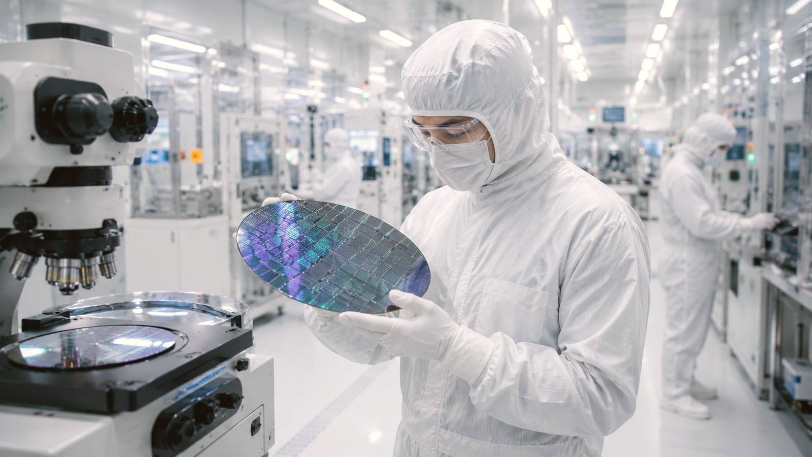
Fab process engineers, equipment specialists, yield engineers, and advanced packaging talent for the US semiconductor build-out. The engineering muscle behind the silicon, placed.
Fab process engineers, equipment specialists, yield engineers, and advanced packaging talent for the US semiconductor build-out. The engineering muscle behind the silicon, placed.
Four converging forces are reshaping US semiconductor manufacturing for the first time in a generation, and turning fab talent into the most contested workforce in domestic industry. This is where AI silicon either ramps on schedule, or quietly slips a node.
CHIPS Act and private capex are bringing fab capacity back onshore at a scale not seen in forty years. TSMC Arizona, Intel Ohio, Samsung Texas, Micron NY, GlobalFoundries, plus equipment suppliers like ASML, Applied Materials, and Tokyo Electron expanding US footprints alongside them.
Advanced packaging (CoWoS, fan-out wafer-level, hybrid bonding) has become the bottleneck for AI silicon. The engineers and equipment specialists who can deliver 2.5D and 3D integration at yield are scarcer than die-level talent.
Process engineers, equipment engineers, yield engineers, fab ramp PMs: the workforce required to operate US fabs at the scale being built doesn't exist domestically at sufficient density. Reshoring without these people is a paper exercise.
CHIPS Act funded fabs and DOE national lab semiconductor programs carry explicit diverse-supplier requirements. WBENC and WOSB put us on small-business sub-tiers primes are obligated to build, channels competitors can't access.
Role clusters where Thunderhawk works specialists who can hit the ground running on fab ramps, equipment installs, and advanced packaging stand-ups.
Process engineers across front-end-of-line and back-end-of-line modules: lithography, etch, deposition, CMP, diffusion, implant. The discipline that determines whether a node yields what the integration team designed.
Tool engineers responsible for the fab's installed base: ASML, Applied Materials, Tokyo Electron, Lam Research, KLA. Up-time, calibration, and qualification specialists who keep the most expensive industrial assets on the planet running.
Yield engineers who chase defects across an unforgiving statistical surface. Failure-mode classification, parametric analysis, defect inspection metrology. The discipline that turns engineering-wafer success into manufacturing-wafer profitability.
Process engineers and integration specialists for CoWoS, fan-out wafer-level packaging, 2.5D and 3D integration, hybrid bonding. The packaging side has become the new bottleneck for AI silicon, and the talent is scarce.
RTL designers, verification engineers, and EDA tool specialists who validate complex chips before they ever reach a fab. Cadence, Synopsys, Siemens EDA fluency, with the methodology discipline that catches the bugs that taping out doesn't.
Program managers and ramp specialists who take a new fab from construction handoff through tool qualification and into production. The orchestration discipline where every week of slip carries ten-figure consequences.
Specific titles we recruit for under this track. Not exhaustive, and calibrated to the scope and stage of your fab, line, or integration program.
Semiconductor work doesn't sit cleanly in one of the seven industries we serve. The talent pool draws on the engineering, equipment, and program-management muscle we already source for adjacent verticals. The track makes the through-line explicit so buyers don't translate between industry and program.
Process, equipment, ramp, yield. The same engineering discipline that delivers complex industrial programs, scaled to the most precise manufacturing on the planet.
See Manufacturing →Rad-hard chips, defense fabs, classified semiconductor work, CMMC-aligned environments. Clearance-aware sourcing where the program demands it.
See Aerospace & Defense →DOE national labs, federal semiconductor research programs, CHIPS Act prime sub-tier panels. The federal layer of the reshore story.
See Public Sector →Network silicon, RF front-end, edge AI accelerators. The chip side of the 5G and edge build-out we already staff.
See Telecom, Media & Entertainment →CHIPS Act funded fabs (TSMC Arizona, Intel Ohio, Samsung Texas, Micron New York, GlobalFoundries) carry diverse-supplier sourcing requirements alongside the primes. WBENC and WOSB are the credentials that put Thunderhawk on the small-business supplier sub-tiers primes are obligated to build out.
DOE national lab semiconductor research awards and federal advanced-manufacturing programs carry parallel diverse-supplier expectations, relevant when the federal and commercial fab build-outs share talent pools.
Where we go deep across fab process, equipment, yield, advanced packaging, design verification, and fab ramp, the roles we fill, and how clients engage, plus how to reach the team.
Tell us where you are: front-end-of-line process, equipment installation, advanced packaging stand-up, or CHIPS Act subcontract support. We'll tell you whether we're the right partner, and we'll be honest if we're not.